

Among the founding scientific schools of Igor Sikorsky Kyiv Polytechnic Institute that have transformed the world of materials science, the school established by outstanding metallurgist, laureate of State Prizes, Honored Scientist and Engineer of Ukraine, Director of Igor Sikorsky Kyiv Polytechnic Institute in 1952–1955, and Academician of the National Academy of Sciences of Ukraine V. Hrydnyev continues to have a significant impact on Ukraine’s scientific and educational fields related to materials science.
Our newspaper previously published an article about the scientific school of the Yevhen O. Paton Educational and Research Institute of Materials Science and Welding, "Physical Materials Science and Technologies of Low-Dimensional Systems," and its current activities under the leadership of Corresponding Member of the National Academy of Sciences of Ukraine Serhii I. Sydorenko (see issues No. 9–10 dated March 8, 2024). Today, this school continues to actively develop in accordance with the conceptual principles of low-dimensional materials science: researchers study structural and phase states with new properties and, based on these studies, develop technologies for functional gradient-layered materials. The achievements of the school's researchers have been recognized seven times with scholarships from the Cabinet of Ministers of Ukraine, twice with scholarships from the President of Ukraine, and with the Borys Paton National Prize of Ukraine. Today, the school can celebrate another stage of recognition: its representatives, Doctor of Physical and Mathematical Sciences I.A. Vladymyrskyi and Doctor of Physical and Mathematical Sciences, Professor S.M. Voloshko, have formed a research team that received funding from the National Research Fund of Ukraine under the "Advanced Science in Ukraine 2026–2028" competition. The team will implement the project "Diffusion Formation of Nanoscale Antiferromagnetic Materials Mnх (Pd, Pt, Ir) with Enhanced Thermal Stability and the Exchange Bias Effect in Functional Structures Based on Them," with funding exceeding UAH 6 million.
Within this project, the team of researchers is developing innovative methods for creating ultrathin metallic composites with layers only a few dozen atoms thick that possess unique characteristics. These materials are critically important for the development of energy-efficient next-generation memory technologies (MRAM) and sensors capable of operating under extreme conditions.
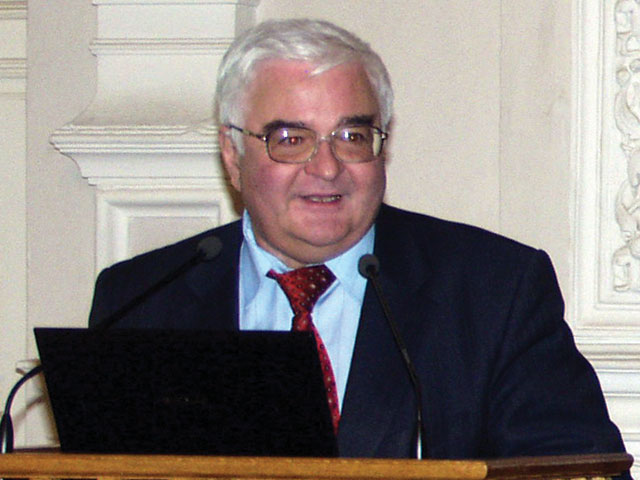 The research team includes not only experienced scientists — Corresponding Member of the National Academy of Sciences of Ukraine S.I. Sydorenko, Professor Yu.M. Makohon, Associate Professor T.I. Verbytska, in addition to Ihor A. Vladymyrskyi and Svitlana M. Voloshko — but also young researchers: Candidates of Sciences and Cabinet of Ministers of Ukraine scholarship holders Andrii K. Orlov and Ivan O. Kruhlov, as well as President of Ukraine scholarship holder, postgraduate student Roman V. Pedan. The involvement of talented young scientists demonstrates the continuity of the scientific school and its confidence in the future.
A correspondent of Kyiv Polytechnic met with the leaders and members of the research team to learn more about the project details, which, in the editorial team's opinion, may be of interest to the academic community of higher education institutions in Ukraine.
– Congratulations on winning the National Research Fund of Ukraine competition! This is a significant achievement, especially for such a fundamental research topic. Could you tell us more about this research?
– Ihor A. Vladymyrskyi The project focuses on developing the scientific foundations for the diffusion formation of thermally stable layered antiferromagnetic (AFM) ordered nanoscale Mn/Me materials (Me – Pd, Pt, Ir) using an approach that we are proposing for the first time. It is based on principles of controlling diffusion rates, including a combination of ionic and thermal effects, changes in the configuration and number of layers, the distribution of mechanical stresses, variation in crystallite size, and the introduction of layers containing alloying elements.
We believe that this approach will make it possible to form a predetermined (ordered) structural-phase state of AFM materials at relatively low heat-treatment temperatures. This is a major advantage, as it provides "more gentle" conditions for the elements of the functional device being created and, accordingly, reduces the likelihood of degradation of its structure and properties.
In particular, we assume that the addition of Au layers will play a regulatory role in the formation of mechanical stresses due to differences in crystal lattice parameters and thermal expansion coefficients of the layer materials.
Our task as physicists and materials scientists is to select such combinations of metal layers with an additional Au layer that will ensure this regulatory effect works in the required direction and with maximum efficiency.
– Terms such as "exchange interaction" or "diffusion formation" in the project title may sound like a kind of spell to non-specialists. To explain this to an audience of a polytechnic university (instrumentation engineers, programmers, energy specialists), could you use some kind of metaphor? For example, "architecture at the atomic level"?
– Ihor A. Vladymyrskyi: When discussing the project, we should talk about a new stage in the development of microelectronics — spin electronics, or spintronics. Devices based on spintronics contain nanoscale layers of magnetic materials in their structure. To describe spintronics in the simplest possible way, we can say that conventional electronics uses only the movement of an electron (the flow of electric current), while spintronics also uses its "rotation" (spin). This significantly expands the possibilities for controlling the states of functional elements and, consequently, the parameters of final devices, making them faster and smaller.
Spintronics is not an alternative to conventional electronics. It is its evolution and its future. Spintronics uses the electron's spin as a magnetic marker, enabling devices that are faster, more compact, and, most importantly, non-volatile.
Therefore, it is indeed possible to say that spintronic effects are elements of an "architecture at the atomic level."
Continuing this metaphor, imagine that we are constructing a multi-story building in which each floor is only a few dozen atoms thick. The thickness of the metal layers we work with is thousands of times smaller than a human hair. Our task is to combine and mix certain metals (for example, manganese with platinum or palladium) in such a way that, within these ultrathin layers, they form a special ordered structure where each atom occupies a precisely defined position. It is this structure that provides the desired antiferromagnetic properties, which ultimately determine the possibility of using these layers in devices of the future.
Usually, achieving such structures requires high temperatures, which complicates the technological processes involved in creating device components. We apply a method of "smart mixing" (diffusion). We not only heat the material but also bombard it with ions and add thin intermediate layers (for example, gold) that act as a kind of catalyst, encouraging atoms to move faster into the positions required.
As for the "exchange interaction effect," it can be explained in simple terms as the mechanism that makes different "floors" of the structure behave as a single whole under the influence of a magnetic field.
– What will this contribute to science in the fundamental sense of the word?
– Svitlana M. Voloshko: The results of our project will help answer the question of how to achieve ordering in a multicomponent low-dimensional material — that is, how to make atoms of different metals occupy specific positions in its structure as required by developers — at relatively low temperatures. These are fundamental insights into how materials can be designed when the size of products made from them approaches the limits of our understanding of the material world.
These results will contribute to the further development of fundamental knowledge in the fields of magnetic phenomena physics and low-dimensional materials science, the discovery of new patterns and effects, and will serve as a foundation for developing new concepts, principles, and methods for creating next-generation antiferromagnetic materials with enhanced thermal stability and improved functional properties. Such materials have broad prospects for practical application in future innovative technologies for the production of spintronics component bases.
– Does the project have practical value for industry?
– Svitlana M. Voloshko: Today, electronics is operating at the limits of its capabilities. Our results will expand these capabilities and provide a foundation for:
– creating elements of non-volatile MRAM (Magnetoresistive Random-Access Memory) — such elements make it possible to retain data when power is switched off and will be more energy efficient;
– developing highly sensitive sensors for medical equipment, navigation systems, and other applications;
– improving the thermal stability of devices that will be able to operate under more demanding conditions without the risk of data loss, since the materials we develop do not change their structure or properties when exposed to increased temperatures.
This is especially important today because by creating such advanced materials, we are effectively forming the component base that spintronics technologies urgently require.
It is also important because the development of technically relevant antiferromagnetic thin-film nanomaterials for a wide range of practical spintronics applications will help reduce Ukraine’s technological gap with developed countries in the field of low-dimensional technologies.
– The project title is quite complex. Does it involve creating new metallic materials or new devices?
– Ihor A. Vladymyrskyi: We are creating "magnetic sandwiches" with atomic-scale thickness, where each layer performs its own specific function. Our innovation lies in how exactly we make atoms of different elements occupy precisely defined positions within these layers.
– You mention the use of gold and ion bombardment — a real 21st-century alchemy! What does this technological "kitchen" look like?
– Svitlana M. Voloshko: In the nanoworld, ordinary laws work differently than they do in bulk materials. To "persuade" atoms, such as manganese and platinum, to occupy their required positions in an ordered structure, we need assistance — ions that bombard the surface and thus "pave the way" for these atoms. Gold layers also provide support by generating additional stresses that, in turn, accelerate atomic movement. This makes it possible to obtain the desired material structure at significantly lower temperatures than usual, thereby saving energy and preserving the integrity of the nanoscale element. This, in turn, determines its stability during operation.
Our technology makes low-dimensional structures more "viable."
– Why is thermal stability, or the "overheating problem" you mentioned, so critical? Aren't modern computers already equipped with cooling systems?
– Ihor A. Vladymyrskyi: The point is that as the size of functional device elements is reduced to the nanoscale, even room temperature may be sufficient to cause a loss of stability. In addition, devices generate heat during operation despite the presence of cooling systems. Our project is aimed at developing materials and structures that can overcome these challenges.
– Can we take a glimpse into the future and imagine the results of your project being used in real-world devices? What significance could this have for Ukraine's economy? Perhaps the young researchers involved in the project would also like to share their perspective, since the future of physical materials science — including materials for spintronics — is in their hands.
– R. V. Pedan: Although we are still at the stage of building the scientific foundation of the technology and developing prototypes, real devices incorporating the materials we are creating are not a matter of some distant future. We are already on the threshold of change. The global market for magnetic memory is growing by 25–30% every year. Ukraine should belong to the group of countries that create intellectual property for the technologies of the near future rather than simply consume them.
This is how the project contributes to Ukrainian science, innovation, and, ultimately, to the country's economy.
– In conclusion, we would like to wish the research team of physicists and materials scientists from the Yevhen O. Paton Institute of Materials Science every success in completing the project and bringing its results into industrial production in Ukraine and across Europe.